| cvs.gedasymbols.org/pcb/bg-image.html | search |
From the command line:
$ pcb --bg-image oldboard.ppm newboard.pcb
From .Xdefaults:
pcb.bg-image: oldboard.ppm
The background image must be a color PPM image, in binary (not ASCII) format. It can be any size, and will be automatically scaled to fit the board, so after you scan the picture, crop it to the edges.
Note that the background image adapts to changes in the board size, so just change the board size after you run pcb.
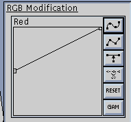
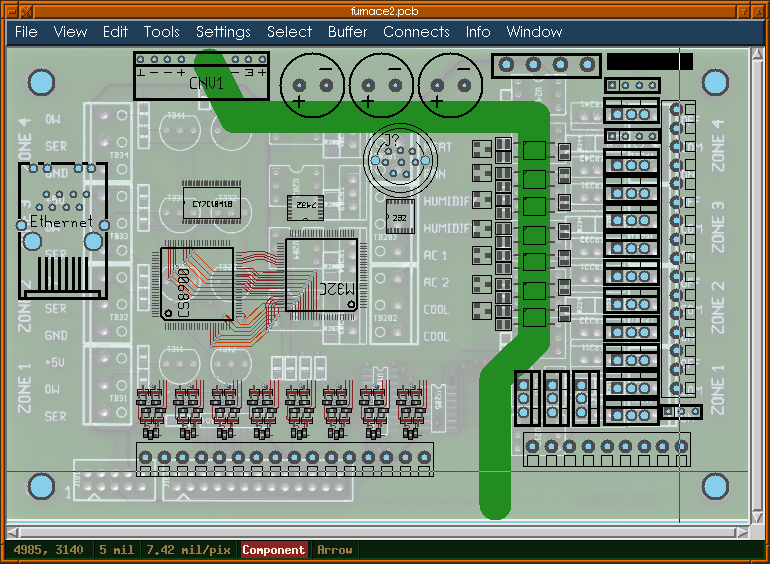
To get the "faded" look (like in the example below), what you do is this: In your image editing program (I use either GIMP or XV), find the "edit curves" option, where you can adjust the transfer curves of the red, green, and blue channels separately. For each color, what you want to do is have a 0 value (black) map to a half-intensity value (usually 128 out of 255). This, effectively, blends your image 50/50 with a solid white. You can use higher black mappings to get a more faded look.
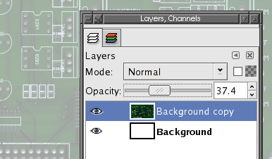
Alternately, in GIMP, use a solid white background layer, and put your image in a separate layer. Now, set your layer to 50% transparency.
 |
 |
| webmaster | delorie software privacy |
| Copyright © 2007 | Updated Sep 2007 |